.jpg)
"인간이 소프트웨어보다 싸졌다"…헤비아 CEO가 던진 'AI 토큰 관리론'
by
2026년 7월 15일

[테크수다 기자 도안구 eyeball@techsuda.com] "코끼리산(Elephant Mountain) 1000계단, 284미터를 올랐다가 한 조각도 잃지 않고 멀쩡히 내려왔다. 그래서 지금 이 자리에 서 있다."
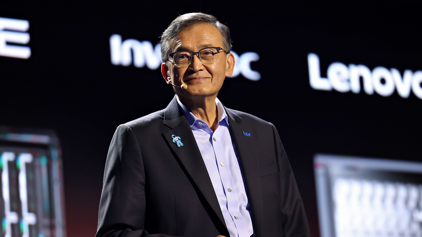
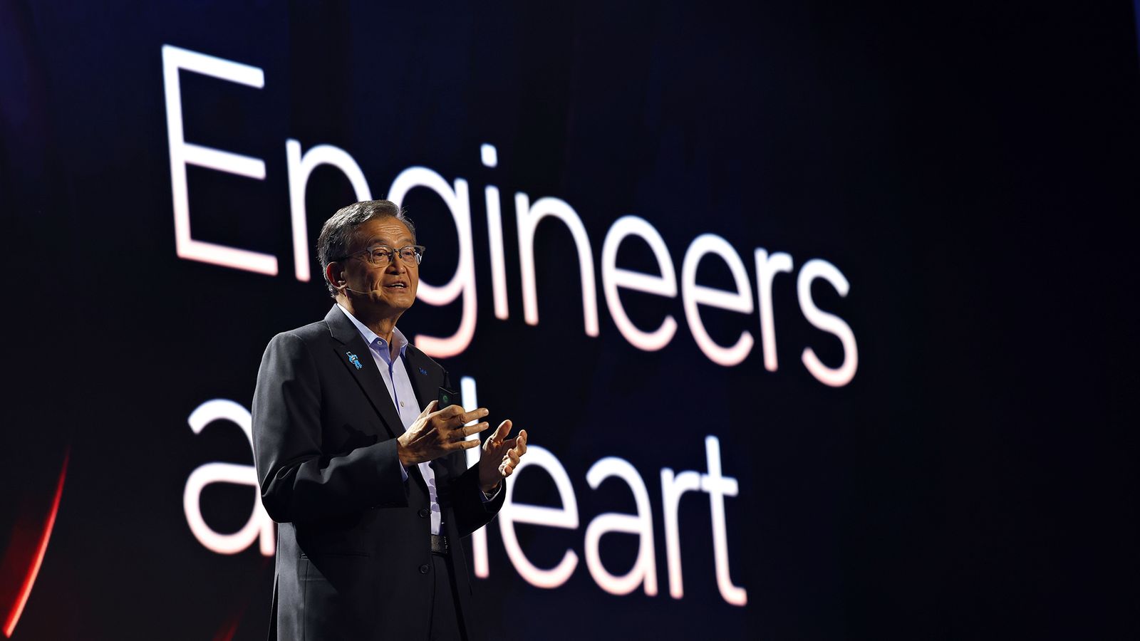
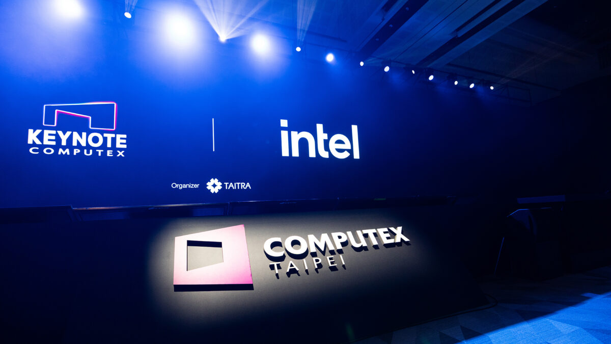
대만 타이베이에서 열린 컴퓨텍스 2026 기조연설. 무대에 오른 립부 탄 인텔 CEO는 농담으로 말문을 열었다. 그러나 그가 곧이어 풀어놓은 이야기는 등산 무용담이 아니라, 한때 컴퓨팅의 대명사였다가 위기에 빠진 회사를 어떻게 다시 일으켜 세우고 있는지에 대한 14개월간의 보고서였다.
▶ 핵심 요약
탄 CEO는 2026년 6월 2일(현지시간) 무대에서 PC, 엣지(edge), 데이터센터, 그리고 새롭게 부상하는 인텔리전스 센터(intelligence center)로 이어지는 4대 컴퓨팅 생태계 전략을 제시하고, 자사 첫 18A(1.8나노급) 공정 기반 제품군의 양산 본격화와 차세대 데이터센터 프로세서 '인텔 제온 6+(Intel Xeon 6+)'를 공개했다. 동시에 구글, 에릭슨을 첫 사례로 맞춤형 실리콘(purpose-built silicon) 시장에 공식 진출한다고 밝혔다. 회사 안팎이 "인텔이 정말 달라졌다"고 느끼기 시작한 변화의 한가운데서, 탄 CEO는 이를 "새로운 인텔(New Intel)"이라는 한 문장으로 압축했다.
이날 연설에는 앨릭스 카투지안(Alex Katouzian) 클라이언트컴퓨팅·피지컬AI그룹 총괄과 케보크 케치키안(Kevork Kechichian) 데이터센터그룹 총괄 등 탄 CEO가 영입한 신임 임원들, 그리고 아라빈드 스리니바스(Aravind Srinivas) 퍼플렉시티(Perplexity) CEO, 로드리고 리앙(Rodrigo Liang) 삼바노바(SambaNova) CEO, 로버트 스미스(Robert F. Smith) 비스타 에퀴티 파트너스(Vista Equity Partners) 회장 등 파트너 기업 수장이 차례로 등장했다. 한 명의 CEO가 주도하던 과거 인텔 키노트와 달리, 무대는 '생태계'를 전면에 내세운 형태로 구성됐다.
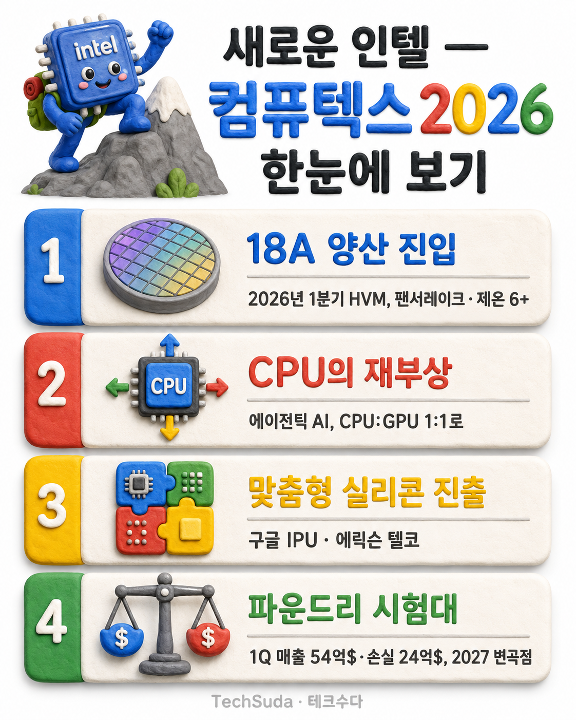
'새로운 인텔'은 탄 CEO가 2025년 3월 취임 이후 추진해온 전환 전략을 가리키는 표현이다. 핵심은 세 가지다. 첫째 엔지니어링 중심 조직으로의 회귀, 둘째 비핵심 사업 정리와 재무 체질 개선, 셋째 자체 제품과 외부 고객을 위한 파운드리·맞춤형 실리콘 사업의 병행 확장이다.
탄 CEO는 무대에서 인텔의 본질을 다시 엔지니어링 기업으로 규정하고, CEO 취임 첫날부터 모든 엔지니어링 조직이 자신에게 직접 보고하도록 체계를 바꿨다고 설명했다. 엔지니어링이 성과를 만들고, 성과가 곧 실행이라는 단순한 명제를 조직 전체에 다시 심겠다는 의도였다. 그는 고객과 파트너가 이미 달라진 인텔을 체감하고 있으며, 회사의 변화는 이제 시작 단계라고 강조했다.
인텔이 스스로 규정한 '4대 컴퓨팅 생태계'는 이 전략의 지도 역할을 한다. 인텔은 매년 수억 개의 시스템온칩(SoC)을 출하하며 실리콘부터 SoC, 시스템, 소프트웨어에 이르는 각 계층에서 파트너 생태계와 긴밀하게 협력하고, 이를 통해 산업 전반에 걸쳐 막대한 가치를 창출한다고 밝혔다.
그 무대를 인텔은 ①개인용 컴퓨터(PC) ②엣지·에이전틱(agentic) AI와 향후 피지컬(physical) AI ③기반 데이터센터 ④미래 디지털 에이전트를 구동할 인텔리전스 센터로 나눴다. 각 생태계마다 워크로드와 애플리케이션에 맞춘 전용 CPU·GPU·ASIC이 필요하며, 인텔이 지금 만들고 있는 실리콘은 사람의 사용뿐 아니라 디지털 에이전트의 사용까지 겨냥한다는 것이 탄 CEO의 설명이다.
| 4대 컴퓨팅 생태계 | 대표 제품·기술 | 컴퓨텍스 2026 핵심 발표 |
|---|---|---|
| PC | 코어 울트라 시리즈 3, 코어 시리즈 3 | 18A 기반 약 400개 디자인 확보, 아크 G3로 휴대용 게이밍 확장 |
| 엣지·피지컬 AI | 시리즈 3 엣지 제품군 | 130개 이상 엣지 디자인, 4000여 엣지 파트너, 피지컬 AI 폼팩터 |
| 기반 데이터센터 | 제온 6+(클리어워터 포레스트) | 18A 첫 서버 칩, 최대 288 E코어, 랙당 약 15만 에이전트 |
| 인텔리전스 센터 | 랙스케일 블루프린트, 분산형 추론 | 삼바노바·폭스콘·비스타와 랙스케일 AI 인프라 실증 |
탄 CEO의 이력은 이 전환 전략의 배경을 설명한다. 1959년 말레이시아에서 태어난 그는 난양대(Nanyang)와 매사추세츠공대(MIT), 샌프란시스코대(USF)를 거쳐 1987년 벤처캐피털 월든 인터내셔널을 설립했다. 그는 반도체 분야의 대표적 투자자로 손꼽히며, 2009년부터 2021년까지 전자설계자동화(EDA) 기업 케이던스를 12년간 이끌면서 경영 능력을 입증했다. 2022년부터 2024년까지 인텔 이사회 멤버로도 활동했다. 업계에서는 그의 인맥과 고객 친화적 경영 스타일을 두고 "반도체 산업에서 그만한 인맥을 가진 사람이 없다"는 평가가 나온다.
탄 CEO는 2025년 3월 18일 인텔 CEO로 취임했다. 컴퓨텍스 2026 연설 시점 기준으로 약 14개월이 지난 셈이다. 그는 자신이 만다린(중국어)을 구사하는 첫 인텔 CEO일 수 있다고 언급하며, 대만 고객·파트너와 술잔을 기울일 수 있는 CEO라는 점도 농담처럼 곁들였다. 이는 단순한 친근함의 표시가 아니라, 인텔 성장의 결정적 기반이었던 대만 PC 생태계와의 관계를 다시 강화하겠다는 메시지였다.
취임 직후부터 탄 CEO는 빠른 실행에 무게를 실었다. 그는 인텔의 재무 상태를 강화하고, 절제된 실행 문화를 정착시키며, 엔지니어링 우선 문화를 되살리는 데 집중했다. 실적에도 변화가 나타나기 시작했다. 인텔은 2025년 4분기 매출 137억 달러로 시장 기대치를 웃돌았고, 2026년 1분기에도 매출 136억 달러로 전년 대비 7% 증가하며 다섯 분기 연속 가이던스를 상회했다. 특히 데이터센터·AI 부문(DCAI)은 1분기에 22% 성장했다.
조직 정비도 과감했다. 인텔은 2025년 7월 이후 약 2만 2000명을 감원해 직원 수를 약 8만 6000명 수준으로 줄였다. 이는 2012년 이후 가장 적은 규모다. 또 비핵심 사업으로 분류한 알테라(Altera)의 지분 51%를 실버레이크(Silver Lake)에 매각해 재무 부담을 덜고 핵심 사업에 집중하는 길을 택했다.
문화적 변화도 동반됐다. 탄 CEO는 한 공개 행사에서 나쁜 소식을 빨리 보고하면 조직 공동의 문제로 함께 풀 수 있지만, 숨기면 개인의 문제가 된다는 취지로 조직 내 솔직함을 강조한 바 있다. 수율과 일정 지연이 반복되며 신뢰를 잃었던 과거를 반복하지 않겠다는 의지의 표현이었다.
탄 CEO가 컴퓨텍스 무대에서 가장 자신 있게 내세운 카드는 18A 공정이다. 18A는 인텔이 자체 개발한 가장 진보된 반도체 노드이자, 미국 영토에서 가동 중인 가장 앞선 제조 공정으로 꼽힌다. 인텔은 2026년 1분기 18A가 고객량 양산(HVM, High Volume Manufacturing)에 진입했다고 밝혔으며, 무대에서 카투지안 총괄은 18A 공정이 이제 본격적인 양산 규모(full scale)에 올랐고 수백 개의 디자인 윈(design win)이 이를 증명한다고 설명했다.
첫 결실은 PC에서 나왔다. 인텔은 올해 1월 CES에서 18A 기반 첫 제품인 코어 울트라 시리즈 3(Core Ultra Series 3, 코드명 팬서레이크)를 선보였다. 빠른 응답성의 CPU, 개선된 GPU, 저전력 신경망처리장치(NPU)를 결합해 프리미엄 모바일 성능과 배터리 수명에서 새 기준을 제시했다는 것이 회사 설명이다. 카투지안 총괄에 따르면 현재 300개 이상의 소비자·상업용 디자인이 출하 중이다.
여기에 인텔은 4월 메인스트림 시장을 겨냥한 코어 시리즈 3(Core Series 3)를 추가로 내놨다. 출시 두 달여 만에 70여 개 디자인을 확보하며, 시리즈 3 제품군 전체로는 단기간에 약 400개 디자인을 모았다. 카투지안 총괄은 이를 "엄청난 규모(massive scale)"라고 표현했다. 그는 PC의 배터리 수명이 사용자의 하루 업무 시간보다 길어야 한다는 점을 강조하며, 경쟁사가 USB-C 포트 하나만 제공하는 것과 달리 인텔 플랫폼은 충분한 포트를 갖췄다고 비교하기도 했다.
성장 속도가 가장 빠른 영역은 휴대용 게이밍이다. 인텔은 코어 울트라 시리즈 3에서 파생한 휴대용 게이밍 전용 GPU '아크 G3(Arc G3)'를 공개했다. 카투지안 총괄은 다수 게임에서 경쟁 제품 대비 40% 빠른 성능을 내고, 같은 성능을 절반의 전력으로 구현하며, 다수 AAA 게임을 1080p 해상도에서 상당수 120fps 이상으로 구동한다고 밝혔다. 아크 G3 기반 기기는 이번 달 내 출시될 예정이다.
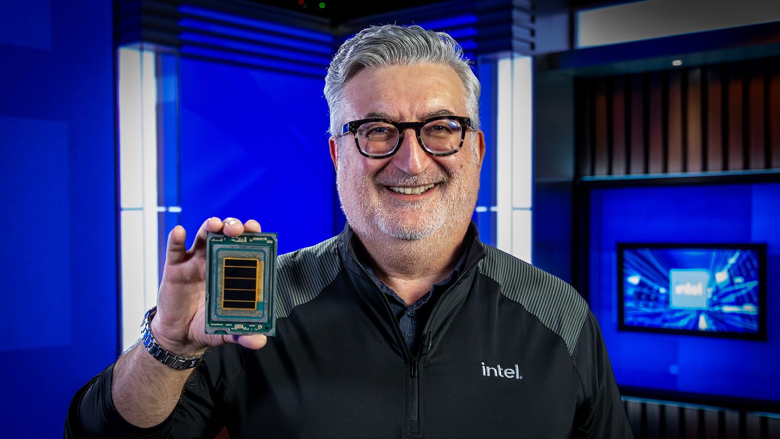
데이터센터에서도 18A는 첫 발을 뗐다. 케치키안 총괄이 공개한 인텔 제온 6+(코드명 클리어워터 포레스트)는 데이터센터 CPU 가운데 처음으로 18A 아키텍처 위에 구축됐다. 최대 288개의 E코어와 576MB에 이르는 거대한 L3 캐시를 갖췄으며, 효율성과 집적도를 앞세워 파트너가 귀중한 공간과 전력을 절약하도록 설계됐다. 케치키안 총괄은 클라우드와 네트워크 인프라의 다음 시대를 위한 리더십 컴퓨트라고 강조했다.
탄 CEO와 케치키안 총괄이 데이터센터 전략의 중심에 놓은 메시지는 분명했다. AI 시대에 CPU가 다시 핵심 엔진으로 돌아온다는 것이다. 인텔은 컴퓨텍스를 앞두고도 AI 워크로드가 컴퓨팅 전반으로 확산되면서 GPU·가속기를 보완하는 AI의 핵심 엔진으로 CPU가 재부상하고 있다는 점을 거듭 부각했다.
논리는 에이전틱 AI의 작동 방식에서 출발한다. 전통적 AI 추론은 프롬프트를 대규모언어모델(LLM)에 넣고 답을 받는 GPU 집약적 과정이다. 반면 에이전틱 AI는 프롬프트가 아니라 목표를 부여받아 계획·실행·반성을 반복하며, 도구를 쓰고 파일을 읽고 쓰며 규칙을 점검한다. 이 과정의 상당 부분이 전통적으로 CPU와 x86의 영역이다. 에이전트가 동시다발적으로 새 에이전트를 생성하며 일을 확장할수록 CPU 수요는 급증한다.
케치키안 총괄은 학습 단계에서 CPU 1개당 GPU 8개 이상이던 비율이 에이전틱 추론으로 옮겨가며 1대 1에 가까운 균형(parity)으로 좁혀지고 있다고 설명했다. 인텔이 공유한 분석에서도 비슷한 진단이 나온다. 벤 바자린(Ben Bajarin) 크리에이티브 스트래티지(Creative Strategies) CEO는 학습 단계에서 일반적이던 CPU 1개당 GPU 4개 비율이 에이전틱 기반 추론 도입과 함께 CPU 1개당 GPU 1개 또는 그 이하로 줄고 있다고 분석했다.
수치는 구체적이다. 인텔 데모에서 제온 6+ 프로세서는 최대 288코어를 갖춰, 2소켓 서버 기준 576코어, 랙 스케일 관점에서는 32U 컴퓨팅 공간에 3만 6864개 코어를 담는다. 케치키안 총괄은 해당 랙이 최대 15만 개의 에이전트를 구동할 수 있다고 밝혔다. 그는 이를 두고 값비싼 GPU의 활용률을 끌어올릴 수 있다는 점에서 최고정보책임자(CIO)들에게 반가운 소식이라고 표현했다.
인텔은 이 비전을 시스템 차원으로 끌어올린 '랙스케일 블루프린트(Rack Scale Blueprints)' 이니셔티브도 소개했다. 개방형 표준 위에서 폭스콘(Foxconn), 삼바노바 등과 협력해 고객이 독점 기술에 종속되지 않고 빠르게 지능형 인프라를 확장하도록 한다는 구상이다. 무대에서는 삼바노바 SN-50 RDU(재구성 가능 데이터플로우 유닛)와 인텔 제온, 엔비디아(NVIDIA) GPU를 결합한 이종(heterogeneous) 분산형 추론도 실증됐다. 같은 모델·같은 프롬프트를 GPU 단독 스택과 GPU·RDU·CPU 분산 스택에 나란히 넣은 결과, 분산 스택이 GPU 단독 대비 2~3배 빠른 결과를 냈다는 것이 리앙 삼바노바 CEO의 설명이다.
이 흐름은 비스타 에퀴티 파트너스의 신규 추론 전용 클라우드 '벡터 코어 컴퓨트(Vector Core Compute, VC2)'로 이어졌다. 스미스 회장은 90개 이상 포트폴리오 기업의 절반 이상이 이미 에이전틱 솔루션으로 전환했고, 7억 5000만 명 이상 사용자를 통해 100억 개가 넘는 에이전트로 환산된다고 밝혔다. 벡터 코어 컴퓨트는 오케스트레이션·실행에 제온, 디코딩에 삼바노바 RDU, 사전처리에 엔비디아 블랙웰(Blackwell) GPU를 쓰는 완전 분산형 추론을 미국 로스앤젤레스 데이터센터에서 시연했고, 투게더 AI(Together.ai)가 첫 상용 고객으로 합류했다.
'새로운 인텔'의 가장 무거운 과제는 파운드리다. 인텔은 자체 제품 제조와 외부 고객 수탁생산을 동시에 추진하는 종합반도체기업(IDM)·파운드리 병행 모델을 고수하고 있다. 그러나 이 사업은 여전히 큰 손실을 낸다. 인텔 파운드리는 2026년 1분기 매출 54억 달러를 기록했지만 영업손실 규모는 약 24억 달러에 달했다. 다만 직전 분기 대비로는 손실이 축소되는 흐름을 보였다.
손실의 한 축은 역설적으로 18A 양산 자체에 있다. 인텔은 1분기 보고서에서 18A로 제조한 고비용 웨이퍼 비중이 늘면서 제품 수익이 줄어 파운드리 손실이 압박받았다고 설명했다. 현재 수율은 출하 물량을 감당할 수준이지만 정상적인 마진을 내기에는 부족하다는 것이 회사 측 인식이다. 인텔은 2026년 말 목표 원가에 도달하고, 2027년에는 업계 평균 수준에 맞추겠다는 계획을 제시했다.
탄 CEO는 그래서 2026년을 '실행의 해'로, 본격적 변곡점을 2027년으로 규정한다. 이 약속의 신뢰도를 좌우하는 것은 결국 외부 고객 확보다. 인텔은 1분기 실적 발표에서 마이크로소프트(Microsoft, 18A 기반 맞춤형 AI 추론 SoC), 브로드컴(Broadcom, 이더넷 스위칭 실리콘) 등을 거명했고, 첫 외부 고객 테이프아웃이 이미 진행됐다고 밝혔다. 회사 운명을 건 18A는 기술 이정표를 넘어, 외부 고객에게 파는 상품 그 자체가 됐다.
회의적 시각도 만만치 않다. 인텔은 18A로 비교적 물량이 적은 팬서레이크 노트북 칩을 만들면서, 물량이 큰 차세대 데스크톱 칩 노바레이크(Nova Lake)의 상당 부분은 대만 TSMC의 N2 공정에 위탁한 것으로 알려졌다. 자사 공정에 대한 인텔 스스로의 선택과 외부 고객에게 내미는 약속 사이의 간극은, 차세대 14A 공정 외부 고객 확보 협상에서 부담으로 작용할 수 있다는 분석이 나온다. 투자 업계에서는 인텔을 두고 "파운드리가 작동하고 대형 고객이 합류하면 주가가 크게 오르지만, 파운드리가 실패하면 다시 저점으로 돌아갈 수 있는, 중간이 없는 이항(binary) 베팅"이라는 평가도 제기됐다.
탄 CEO가 이날 던진 또 하나의 승부수는 맞춤형 실리콘 사업 진출이다. 그는 반도체 설계 베테랑이자 맞춤형 실리콘 팀을 이끄는 스리니바산 아이옌가(Srinivasan Iyengar) 중앙엔지니어링 총괄을 무대로 불러 두 건의 성과를 공개했다.
첫째는 하이퍼스케일러 영역이다. 구글과 인텔은 인텔이 인프라처리장치(IPU, Infrastructure Processing Unit)를 공급하는 파트너십을 맺었다. IPU는 네트워킹·스토리지·보안 기능을 호스트 CPU에서 분리해 처리하는 ASIC 기반 가속기로, 하이퍼스케일러 성능에 핵심적인 실리콘이다. 아이옌가 총괄은 이 IPU가 단순 개발 단계를 넘어 이미 설계·배포 단계에 들어섰다고 강조했다. 양사는 이미 2021년 '마운트에반스(Mount Evans)'라는 첫 IPU로 협력을 시작했고, 2026년 4월 다세대 제온 공급과 IPU 공동개발 확대를 골자로 한 다년 협약을 체결한 바 있다.
둘째는 텔코 시장이다. 또 다른 대형 고객인 에릭슨이 인텔과 손잡고, 인텔이 차세대 인프라 실리콘을 글로벌 규모로 공급한다. 아이옌가 총괄은 맞춤형 실리콘이 지난 10여 년간 하이퍼스케일러들이 그 잠재력을 입증해온 고성장 영역이라며, 커스텀 실리콘이 곧 게임의 핵심인 타이베이 컴퓨텍스에서 인텔이 이 시장에 공식 진입한다고 선언하기에 적합한 무대라고 말했다.
맞춤형 실리콘 진출은 인텔의 약점을 정면으로 겨냥한 카드다. 그동안 인텔은 클라우드 사업자들이 자체 칩을 설계하는 흐름 속에서 존재 의미에 대한 의문에 시달렸다. 세계 최대 클라우드 사업자 중 하나인 구글과 깊은 맞춤형 실리콘 관계를 유지한다는 사실은, 인텔의 파운드리·설계 역량이 인프라 핵심 워크로드에서 여전히 경쟁력 있음을 보여주는 신호로 해석된다.
탄 CEO는 맞춤형 실리콘을 산업 버티컬로 확장하는 그림도 펼쳤다. PC, 엣지, 데이터센터를 떠받치는 기반 IP로 그는 x86 아키텍처를 꼽았다. 시장조사기관 IDC를 인용해 2030년까지 설치되는 서버 10대 중 8대가 x86 기반일 것이라고 전망하며, 1978년 8086에서 시작된 x86의 리더십이 계속된다고 강조했다. 인텔은 성능에 최적화된 P코어와 효율에 최적화된 E코어 두 종류의 플래그십 CPU 코어를 앞세워, 가장 연산 집약적인 워크로드가 x86에서 가장 잘 돌도록 하겠다고 밝혔다.
이 기반 위에서 인텔은 다양한 산업 파트너를 소개했다. 뇌에서 영감을 받은 컴퓨팅 분야에서는 에코 뉴로테크놀로지스(Echo Neurotechnologies)와 협력한다. UCSF 신경외과의이자 공동창업 CEO인 에디 청(Eddie Cheng)은 인간 대뇌피질이 실시간으로 언어를 연산하는 방식을 처음으로 그 해상도에서 연구할 수 있게 됐다며, 뇌 활동 자체로 학습한 새로운 알고리즘으로 생물학적 연산의 효율에 다가가는 한편 언어를 잃은 사람들의 말을 되찾는 도구를 함께 개발한다고 소개했다.
생명과학에서는 그린스톤 바이오사이언스(Greenstone Biosciences)와 손잡는다. 스탠퍼드 심혈관연구소장이자 공동창업 CEO인 조셉 우(Joseph Wu)는 단 10cc의 혈액으로 환자와 유전적으로 동일한 뇌·심장·간·신장 등 오가노이드를 만드는 세계 최대 규모의 유도만능줄기세포 바이오뱅크를 구축했다고 밝혔다. 그는 인텔의 컴퓨팅과 그린스톤의 인간 유전학·생물학을 결합해 신약 개발을 더 빠르고 저렴하게 검증하겠다고 설명했다.
산업·인프라 영역에서는 지멘스(Siemens)와 히타치(Hitachi)가 합류했다. 롤란트 부슈(Roland Busch) 지멘스 CEO는 설계부터 제조, 지멘스 제품에 내장되는 칩에 이르기까지 밸류체인 전반으로 협력을 확대한다고 밝혔다. 도쿠나가 도시아키(Toshiaki Tokunaga) 히타치 CEO는 인텔의 첨단 컴퓨팅과 히타치의 산업 역량을 결합해 기업과 사회 모두에 도움이 되는 지능형 솔루션을 만들겠다고 말했다. 시스템 통합 분야에서는 폭스콘 최고제품책임자 제리 샤오(Jerry Xiao)가 무대에 올라 인텔 제온 기반 랙스케일 AI 인프라 공동 개발 계획을 발표했다.
이로써 인텔은 PC와 게이밍 같은 소비자 영역에서, 데이터센터와 텔코 같은 인프라 영역을 거쳐, 뇌과학과 바이오 같은 첨단 연구 영역까지 자사 실리콘을 펼치는 그림을 한 자리에서 보여줬다. 하나의 칩을 모든 곳에 파는 방식이 아니라, 워크로드가 전략 자산이 된 시대에 고객별로 맞춤형 실리콘을 제공하겠다는 전략의 시각화였다.
탄 CEO가 굳이 등산 이야기로 연설을 연 데에는 이유가 있었다. 그에게 대만은 인텔의 부활을 이야기하기에 가장 상징적인 장소다.
그는 약 40년 전 대만 반도체 산업의 태동에 직접 관여한 인연을 회고했다. 당시 리궈딩(K.T. Li, 李國鼎) 장관의 초청으로 대만에 벤처캐피털 개념의 토대를 놓았고, 투자자가 손실의 20%는 나누지 않되 이익의 20%를 공유하는 독특한 구조의 벤처펀드를 설립했다고 설명했다. 비슷한 시기에 텍사스인스트루먼츠(TI) 출신 모리스 창(Morris Chang)이 대만으로 돌아와 TSMC를 세웠고, 신주과학단지(Hsinchu Science Park)를 중심으로 대만은 설계부터 제조까지 아우르는 '실리콘 아일랜드(Silicon Island)'로 성장했다. 탄 CEO는 미국 실리콘밸리의 탄생과 같은 야망과 사고방식이 바다 건너 대만에서도 반도체 제조의 불꽃을 일으켰다고 평가했다.
이 회고는 단순한 향수가 아니다. 대만 PC 생태계는 인텔의 성장과 성공에 결정적 역할을 했고, 탄 CEO는 지난해 인텔의 대만 진출 40주년을 이 자리에서 기념하기도 했다. 자체 공정과 외부 파운드리, 그리고 OEM·ODM 파트너망이 그 어느 때보다 중요해진 지금, 인텔은 자신을 키운 대만 생태계와의 관계를 다시 협력의 핵심 축으로 세우고 있다. 마무리 무대에서 인텔이 맥라렌 레이싱(McLaren Racing)의 공식 컴퓨트 파트너임을 알리는 영상으로 연설을 닫은 것도, 경주가 끝나지 않았고 엔지니어링은 멈추지 않는다는 메시지를 담았다.
향후 전망은 탄 CEO 스스로 그은 시간표에 달려 있다. 그는 컴퓨텍스 무대에서 1년 전 CEO로 합류하며 팀에 새로운 인텔을 함께 만들자고 요청했고, 인텔은 과거에 얽매이지 않고 멋진 무언가를 만들고 있다고 말했다. 18A 양산, 첨단 패키징 이정표, 파운드리 고객 확대, 전 컴퓨팅 플랫폼을 아우르는 신규 SoC가 동시에 진행 중인 '전환의 해'라는 것이다.
문제는 선언이 아니라 숫자다. 인텔은 18A 수율을 끌어올려 마진을 정상화하고, 14A에 대형 외부 고객을 붙이며, 파운드리 손실을 줄여야 한다. 이 세 가지가 2026년 안에 가시화되지 않으면 '새로운 인텔'의 서사는 다시 의문에 부딪힐 수 있다. 반대로 약속이 지켜진다면, 컴퓨텍스 2026은 인텔이 한 발 앞서 변곡점을 예고한 무대로 기록될 것이다. 코끼리산 정상에서 한 조각도 잃지 않고 내려왔다던 탄 CEO의 농담이, 14개월 뒤 어떤 결과로 돌아올지 지켜볼 일이다.
Q1. '새로운 인텔'은 정확히 무엇을 의미하나?
탄 CEO가 2025년 3월 취임 이후 추진해온 전환 전략을 압축한 표현이다. ①엔지니어링 중심 조직으로의 회귀 ②비핵심 사업 정리와 재무 체질 개선 ③자체 제품과 외부 고객을 동시에 겨냥한 파운드리·맞춤형 실리콘 사업 확장이 핵심 골격이다.
Q2. 18A 공정이 왜 이번 연설의 핵심인가?
18A는 인텔이 자체 개발한 가장 진보된 노드로, 2026년 1분기 고객량 양산에 진입했다. 코어 울트라 시리즈 3(PC)와 제온 6+(서버)가 모두 18A 위에 올라 있어, 18A의 양산과 수율은 인텔 전체 반등 전략의 성패를 가르는 기준점이 된다.
Q3. 'AI 시대에 CPU가 다시 중요해진다'는 주장의 근거는?
에이전틱 AI는 목표를 부여받아 계획·실행·반성을 반복하며 도구 사용·파일 처리·규칙 점검 등 CPU 영역의 작업을 대량으로 수행한다. 이 때문에 학습 단계에서 CPU 1개당 GPU 4~8개이던 비율이 에이전틱 추론에서는 1대 1에 가깝게 좁혀지고 있다는 것이 인텔과 시장 분석가들의 진단이다.
Q4. 인텔 파운드리는 흑자로 돌아섰나?
아직 아니다. 2026년 1분기 파운드리는 매출 54억 달러에 영업손실 약 24억 달러를 기록했다. 18A 고비용 웨이퍼 비중이 손실을 키운 측면이 있으며, 인텔은 2026년 말 목표 원가 도달, 2027년 업계 평균 마진 달성을 목표로 제시했다.
Q5. 인텔의 반등을 가로막을 수 있는 위험은?
18A 수율과 마진 개선이 계획대로 진행될지, 차세대 14A 공정에 대형 외부 고객을 확보할 수 있을지가 관건이다. 인텔이 물량 큰 데스크톱 칩(노바레이크)을 TSMC에 위탁한 점은 자체 공정 신뢰도에 대한 의문으로 이어질 수 있다. 업계는 인텔을 '중간이 없는 이항 베팅'으로 평가한다.
[Seoul = Techsuda eyeball@techsuda.com]
▶ Key Takeaways
[Seoul = TechSuda eyeball@techsuda.com] "I climbed Elephant Mountain—1,000 steps, 284 meters—and came back down in one piece. So here I am."
That was how Lip-Bu Tan, CEO of Intel, opened his keynote at Computex 2026 in Taipei. The joke was about a hike. What followed was not a travelogue but a 14-month progress report on how he is trying to lift a company that once defined computing—and then fell into crisis—back onto its feet.
On June 2, 2026 (local time), Tan laid out a strategy spanning four computing ecosystems—the PC, the edge, the data center, and the emerging "intelligence center"—and unveiled the broad rollout of Intel's first products built on the 18A (1.8nm-class) process, along with the next-generation Intel Xeon 6+ data-center processor. He also announced Intel's formal entry into the purpose-built silicon market, citing Google and Ericsson as its first customers. At the center of a shift that has both insiders and outsiders saying "Intel really has changed," Tan compressed the message into a single phrase: the "New Intel."
The keynote featured executives Tan has recruited—Alex Katouzian, head of the Client Computing and Physical AI Group, and Kevork Kechichian, head of the Data Center Group—alongside partner CEOs including Perplexity's Aravind Srinivas, SambaNova's Rodrigo Liang, and Vista Equity Partners chairman Robert F. Smith, who appeared in turn. Unlike past Intel keynotes anchored by a single CEO, the stage was built around an "ecosystem."
"New Intel" is shorthand for the transformation strategy Tan has pursued since taking over in March 2025. It rests on three pillars: a return to an engineering-first organization; the cleanup of non-core businesses and the strengthening of the balance sheet; and the parallel expansion of a foundry and custom-silicon business serving both Intel's own products and external customers.
On stage, Tan redefined Intel as, at its heart, an engineering company, and explained that from his first day as CEO he restructured reporting lines so that all engineering organizations report directly to him. His intent was to re-instill a simple proposition across the company: engineering drives performance, and performance is execution itself. Customers and partners, he said, already sense a different Intel, and the company is only getting started.
Intel's self-defined "four computing ecosystems" serve as the map for this strategy. The company ships hundreds of millions of systems-on-chip (SoCs) each year, working closely with its partner ecosystem across every layer—from silicon to SoC to system to software—generating enormous value across industries. Intel divides that arena into the personal computer (PC); the edge, agentic AI, and eventually physical AI; foundational data centers; and the intelligence centers that will power the digital agents of the future. Each ecosystem, Tan argued, needs purpose-built CPUs, GPUs, and ASICs tailored to specific workloads, and the silicon Intel is building now is aimed not only at human use but at the use of digital agents as well.
| Four Computing Ecosystems | Key Products / Tech | Computex 2026 Highlights |
|---|---|---|
| PC | Core Ultra Series 3, Core Series 3 | ~400 designs on 18A; Arc G3 expands into handheld gaming |
| Edge / Physical AI | Series 3 edge lineup | 130+ edge designs, 4,000+ edge partners, physical-AI form factors |
| Foundational Data Center | Xeon 6+ (Clearwater Forest) | First 18A server chip, up to 288 E-cores, ~150,000 agents per rack |
| Intelligence Center | Rack Scale Blueprints, disaggregated inference | Rack-scale AI infrastructure demos with SambaNova, Foxconn, Vista |
Tan's background explains the logic behind this strategy. Born in Malaysia in 1959, he studied at Nanyang University, MIT, and the University of San Francisco before founding the venture-capital firm Walden International in 1987. Widely regarded as one of the most prominent investors in semiconductors, he proved his operating chops by running the electronic-design-automation (EDA) company Cadence Design Systems for 12 years, from 2009 to 2021, and served on Intel's board from 2022 to 2024. In the industry, his network and customer-centric style draw remarks that "no one in semiconductors has a Rolodex like his."
Tan became Intel CEO on March 18, 2025—roughly 14 months before the Computex 2026 keynote. He noted he may be the first Intel CEO who speaks Mandarin, and joked that he is also a CEO who can share a drink with Taiwan's customers and partners. The remarks were less about charm than a message: a determination to rebuild ties with the Taiwanese PC ecosystem that was decisive to Intel's rise.
From the outset, Tan emphasized fast execution. He focused on strengthening Intel's finances, instilling disciplined execution, and reviving an engineering-first culture. The results began to show. Intel posted fourth-quarter 2025 revenue of $13.7 billion, beating expectations, and first-quarter 2026 revenue of $13.6 billion, up 7% year over year—its fifth straight quarter of beating guidance. The Data Center and AI (DCAI) segment grew 22% in the first quarter.
The organizational cleanup was aggressive. Intel cut roughly 22,000 jobs after July 2025, bringing headcount to about 86,000—the smallest since 2012. It also sold a 51% stake in Altera, deemed non-core, to Silver Lake, easing financial strain and concentrating on the core business.
A cultural shift accompanied the moves. At a public event, Tan stressed candor inside the organization, framing it roughly this way: if you tell me the bad news quickly, it becomes our shared problem to solve; if you hide it, it becomes your problem. It was a vow not to repeat a past marred by recurring yield and schedule slips that eroded trust.
The card Tan played with the most confidence at Computex was the 18A process. 18A is Intel's most advanced internally developed node and is described as the most advanced semiconductor manufacturing process operating on U.S. soil. Intel said 18A entered high-volume manufacturing (HVM) in the first quarter of 2026, and on stage Katouzian explained that 18A is now at full scale, with hundreds of design wins to prove it.
The first fruit came in the PC. In January, at CES, Intel unveiled its first 18A-based product, the Core Ultra Series 3 (codenamed Panther Lake). Combining a fast-responding CPU, an improved GPU, and a low-power neural processing unit (NPU), it set a new bar for premium mobile performance and battery life, the company said. According to Katouzian, more than 300 consumer and commercial designs are now shipping.
Intel then added the Core Series 3, aimed at the mainstream market, in April. Within roughly two months it racked up more than 70 designs, bringing the full Series 3 lineup to about 400 designs in a short span. Katouzian called it "massive scale." He stressed that a PC's battery should outlast the user's workday, and contrasted Intel's ample port selection with rivals that offer only a single USB-C interface.
The fastest-growing area is handheld gaming. Intel unveiled the Arc G3, a handheld-gaming GPU derived from the Core Ultra Series 3. Katouzian said it runs more than 40% faster than competing products across many games, delivers the same performance at half the power, and runs many AAA games at 1080p, with a good number above 120 fps. Devices based on the Arc G3 are due out later this month.
The data center took its first 18A step as well. The Intel Xeon 6+ (codenamed Clearwater Forest), unveiled by Kechichian, is the first data-center CPU built on the 18A architecture. It packs up to 288 E-cores and a massive 576 MB of L3 cache, and is engineered for efficiency and density so partners can save precious space and power. Kechichian called it leadership compute for the next era of cloud and network infrastructure.
The message Tan and Kechichian placed at the center of their data-center pitch was clear: in the age of AI, the CPU returns as a core engine. Heading into Computex, Intel had repeatedly underscored the CPU's resurgence as a critical engine for AI that complements GPUs and accelerators as AI workloads spread across computing.
The logic starts with how agentic AI works. Traditional AI inference feeds a prompt into a large language model (LLM) and returns an answer—a GPU-intensive process. Agentic AI, by contrast, is given goals rather than prompts and loops through planning, acting, and reflecting, using tools, reading and writing files, and checking rules. Much of that work is traditionally the domain of the CPU and x86. As agents scale up by spawning new agents to work concurrently, CPU demand rises sharply.
Kechichian explained that the ratio of one CPU to eight or more GPUs during training is narrowing toward parity—closer to one-to-one—as workloads shift to agentic inference. Analysis Intel shared points the same way. Ben Bajarin, CEO of Creative Strategies, noted that the roughly four-GPU-per-CPU ratio common in training is shrinking to about one GPU per CPU, or less, with the arrival of agentic-based inference.
The figures are concrete. In Intel's demo, the Xeon 6+ offers up to 288 cores—576 cores in a two-socket server, and 36,864 cores within 32U of rack-scale compute space. Kechichian said such a rack can run up to 150,000 agents. He framed it as good news for CIOs, since it lets their very expensive GPUs see higher utilization.
Intel also introduced the system-level "Rack Scale Blueprints" initiative, working with partners such as Foxconn and SambaNova on open standards so customers can scale intelligent infrastructure quickly without proprietary lock-in. On stage, a heterogeneous disaggregated-inference setup combining SambaNova's SN-50 RDU (reconfigurable dataflow unit) with Intel Xeon and NVIDIA GPUs was demonstrated. Running the same model and the same prompt side by side against a GPU-only stack, the disaggregated stack delivered results two to three times faster than GPUs alone, according to Liang of SambaNova.
That thread extended to Vista Equity Partners' new inference-only cloud, Vector Core Compute (VC2). Smith said more than half of Vista's 90-plus portfolio companies have already converted to agentic solutions, translating—across more than 750 million users—into over 10 billion agents. Vector Core Compute demonstrated fully disaggregated inference—using Xeon for orchestration and execution, SambaNova RDUs for decoding, and NVIDIA Blackwell GPUs for prefill—running live in a Los Angeles data center, with Together.ai signing on as the first commercial customer.
The heaviest task facing the "New Intel" is the foundry. Intel sticks to an integrated-device-manufacturer (IDM)-plus-foundry model, building its own products while also taking on external customers. But the business still loses heavily. Intel Foundry posted first-quarter 2026 revenue of $5.4 billion against an operating loss of roughly $2.4 billion, though the loss narrowed from the prior quarter.
One driver of the loss is, paradoxically, 18A's own ramp. Intel said in its first-quarter filing that a higher mix of costly wafers manufactured on 18A reduced product profit and pressured the foundry loss. Current yields can support shipment volumes but not normal margins, the company acknowledged. Intel set a goal of reaching target costs by the end of 2026 and aligning with industry-average margins in 2027.
That is why Tan frames 2026 as the "year of execution," with the real inflection point in 2027. The credibility of that promise ultimately turns on landing external customers. In its first-quarter earnings, Intel named customers including Microsoft (a custom AI inference SoC on 18A) and Broadcom (Ethernet switching silicon), and said the first external-customer tape-outs are already through the door. 18A, on which the company's fate rests, has become more than a technology milestone—it is the product Intel is selling.
Skepticism runs deep, however. Intel is using 18A for the relatively low-volume Panther Lake notebook chips, while a large share of the higher-volume next-generation desktop chip, Nova Lake, is reportedly outsourced to TSMC's N2 process. The gap between Intel's own manufacturing choices and the promises it makes to external customers could weigh on negotiations for the next-generation 14A node. Investors have described Intel as a "binary bet with no middle ground": if the foundry works and big customers commit, the stock re-rates sharply; if it fails, it could revisit prior lows.
Tan's other big wager was Intel's entry into the custom-silicon business. He brought on stage Srinivasan Iyengar, head of Central Engineering and leader of the purpose-built silicon team, to unveil two wins.
The first is in the hyperscaler arena. Google and Intel have formed a partnership in which Intel supplies the infrastructure processing unit (IPU)—an ASIC-based accelerator that offloads networking, storage, and security functions from host CPUs, a piece of silicon vital to hyperscaler performance. Iyengar stressed that the IPU is past mere development and already in the design-and-deployment stage. The two companies first began collaborating on an IPU—"Mount Evans"—in 2021, and in April 2026 signed a multiyear agreement covering multi-generation Xeon supply and expanded IPU co-development.
The second is the telecom market. Ericsson, another marquee customer, has partnered with Intel to have Intel supply next-generation infrastructure silicon at global scale. Iyengar called custom silicon a high-growth space whose potential hyperscalers have proven over the past decade, and said there was no better stage than Taipei's Computex—where custom silicon is the name of the game—to declare Intel's official entry into the market.
The custom-silicon push targets one of Intel's vulnerabilities head-on. For years, Intel has faced questions about its relevance as cloud providers increasingly design their own chips. Maintaining a deep custom-silicon relationship with one of the world's largest cloud operators signals that Intel's foundry and design capabilities remain competitive for infrastructure-critical workloads.
Tan also sketched a picture of extending custom silicon across industry verticals. As the foundational IP underpinning the PC, edge, and data center, he pointed to the x86 architecture. Citing IDC, he projected that eight of every ten servers installed through 2030 will be x86-based, and stressed that the leadership begun with the 8086 in 1978 continues. Intel leads with two flagship CPU cores—P-cores optimized for performance and E-cores optimized for efficiency—and pledged to ensure the most compute-intensive workloads run best on x86.
On that foundation, Intel introduced a range of industry partners. In brain-inspired computing, it is working with Echo Neurotechnologies. Eddie Cheng, a UCSF neurosurgeon and co-founder and CEO, said that for the first time researchers can study how the human cortex computes language in real time at the resolution where computation actually happens, and that the partnership develops new algorithms trained on brain activity itself—approaching the efficiency of biological computation while also building tools to restore speech to people who have lost it.
In life sciences, Intel is teaming with Greenstone Biosciences. Joseph Wu, director of the Stanford Cardiovascular Institute and co-founder and CEO, said the company has built the world's largest biobank of induced pluripotent stem cells, capable of producing organoids—brain, heart, liver, kidney, and more—genetically identical to a patient from just 10 cc of blood. He explained that combining Intel's computing with Greenstone's human genetics and biology will let them test medicines faster and at lower cost.
In industry and infrastructure, Siemens and Hitachi joined in. Siemens CEO Roland Busch said the companies are expanding collaboration across the entire value chain—from design to manufacturing to the chips embedded in Siemens products. Hitachi CEO Toshiaki Tokunaga said the partnership will pair Intel's advanced computing with Hitachi's industrial strength to create intelligent solutions that benefit both businesses and society. On the systems-integration front, Foxconn Chief Product Officer Jerry Xiao took the stage to announce plans to co-develop rack-scale AI infrastructure built on Intel Xeon.
With that, Intel showed, in a single sitting, how its silicon reaches from consumer arenas like the PC and gaming, through infrastructure domains like the data center and telecom, to cutting-edge research fields like neuroscience and biotech. It was a visualization of a strategy that no longer sells one chip everywhere, but offers purpose-built silicon customer by customer in an era when workloads have become strategic assets.
There was a reason Tan opened with a hiking story. For him, Taiwan is the most symbolic place to talk about Intel's revival.
He recalled his direct involvement in the birth of Taiwan's semiconductor industry some 40 years ago. At the invitation of Minister K.T. Li (李國鼎), he laid the groundwork for the concept of venture capital in Taiwan, setting up a venture fund with an unusual structure in which investors shared 20% of profits without sharing 20% of losses. Around the same time, Morris Chang, who came from Texas Instruments (TI), returned to Taiwan and founded TSMC, and—centered on the Hsinchu Science Park—Taiwan grew into a "Silicon Island" spanning design to manufacturing. Tan said the same ambition and mindset that created Silicon Valley sparked the rise of semiconductor manufacturing across the ocean in Taiwan.
The recollection is more than nostalgia. The Taiwanese PC ecosystem was decisive to Intel's growth and success, and last year Tan marked Intel's 40th anniversary in Taiwan from this same stage. With internal process, external foundry, and a network of OEM and ODM partners more important than ever, Intel is reestablishing its relationship with the very ecosystem that nurtured it as a core axis of collaboration. Closing the keynote with a video declaring Intel the official compute partner of McLaren Racing carried the message that the race is not over and engineering never stops.
The outlook hinges on the timetable Tan drew himself. On the Computex stage he said that when he joined as CEO a year ago, he challenged his team to build a new Intel together, and that Intel is not held back by its past but is building something wonderful. It is a "year of transformation," with 18A volume production, advanced-packaging milestones, an expanding foundry customer base, and new SoCs across every computing platform all advancing at once.
The issue, though, is not declarations but numbers. Intel must raise 18A yields to normalize margins, attach major external customers to 14A, and shrink foundry losses. If those three do not materialize within 2026, the "New Intel" narrative could face renewed doubt. If the promises hold, however, Computex 2026 will be remembered as the stage where Intel signaled its inflection point a step ahead. Whether Tan's joke—about descending Elephant Mountain in one piece—returns as a fitting metaphor 14 months from now remains to be seen.
Q1. What exactly does "New Intel" mean?It is shorthand for the transformation strategy Tan has pursued since taking over in March 2025: (1) a return to an engineering-first organization, (2) cleanup of non-core businesses and a stronger balance sheet, and (3) expansion of a foundry and custom-silicon business serving both Intel's own products and external customers.
Q2. Why is the 18A process the heart of this keynote?
18A is Intel's most advanced internally developed node, and it entered high-volume manufacturing in Q1 2026. Both the Core Ultra Series 3 (PC) and Xeon 6+ (server) are built on 18A, so 18A's ramp and yields are the benchmark for the success or failure of Intel's entire turnaround.
Q3. What is the basis for the claim that "the CPU matters again in the AI era"?
Agentic AI is given goals rather than prompts and loops through planning, acting, and reflecting—performing CPU-domain work such as tool use, file handling, and rule-checking in large volumes. As a result, the four-to-eight GPUs per CPU common in training is narrowing toward one-to-one in agentic inference, according to Intel and market analysts.
Q4. Has Intel's foundry turned profitable?
Not yet. In Q1 2026 the foundry posted $5.4 billion in revenue against an operating loss of about $2.4 billion. A higher mix of costly 18A wafers enlarged the loss, and Intel targets reaching its cost goals by the end of 2026 and industry-average margins in 2027.
Q5. What risks could derail Intel's recovery?
Whether 18A yields and margins improve on plan, and whether Intel can land major external customers for the next-generation 14A node. Outsourcing the high-volume desktop chip (Nova Lake) to TSMC could raise doubts about confidence in its own process. The industry calls Intel a "binary bet with no middle ground."
[Seoul = Techsuda eyeball@techsuda.com]
테크가 전 산업 영역에 스며드는 소식에 관심이 많다. 1999년 정보시대 PCWEEK 테크 전문지 기자로 입문한 후 월간 텔레닷컴, 인터넷 미디어 블로터닷넷 창간 멤버로 활동했다. 개발자 잡지 마이크로소프트웨어 편집장을 거쳐 테크수다를 창간해 지금까지 활동하고 있다. 태블릿을 가지고 얼굴이 꽉 찬 방송, 스마트폰을 활용한 현장 라이브를 한국 최초로 진행했다.